MARKET OVERVIEW
The Global Plasma Dicing Systems for Semiconductor market is an increasingly important part of the semiconductor industry focused on advanced wafer dicing technology. Plasma dicing is one of the relatively new approaches of dicing technology that has emerged in recent years and is considered cleaner as well as much more efficient when compared to traditional blade dicing in regard to individual semiconductor chip separation from wafers. Whereas the design of chips becomes more complex and fragile in the semiconductors industry, there is a real need for non-destructive dicing techniques with high accuracy. Today, plasma dicing has thus emerged as an important technology to cater to these needs in semiconductor manufacturing.
Dicing in semiconductor manufacturing is one of the last stages in the process, but the very important role it plays in preserving the delicate ICs on each chip as intact and undamaged. The main problem with mechanical blade dicing is that this method tends to damage the wafers easily, thus introducing defects or contaminating them. Moreover, the geometry of chips continue to shrink while there is an increasing demand for small but powerful devices. In plasma dicing, chemical reactions separate the chips hence there is no chance of their cracking or contamination.
It is the shifting trend of how manufacturers in the semiconductor industry deal with wafer dicing. With plasma etching, manufacturers can produce cleaner cuts with less debris, thus higher yields and chips. It cuts close when the chips get too small-there is less room for error. This plasma dicing process also provides a means to produce much more versatile designs in a chip; this aspect can facilitate new configurations and layouts, which are relatively easy to explore in ways that cannot come into play with traditional dicing methods that place restrictions.
Another benefit of plasma dicing is that it scales up much better. As semiconductor fabrication is moving towards greater wafer sizes, plasma dicing systems are very important in handling the wafers effectively. The Global Plasma Dicing Systems for Semiconductor market will continue to grow as manufacturers shift toward larger wafers to gain production efficiencies. Its ability to handle greater-sized wafers without losing precision or quality will be a prominent reason for its adoption.
There would also be an upsurge in demand for Global Plasma Dicing Systems for Semiconductors driven by advanced packaging solutions. As the maturity of 5G, IoT, and artificial intelligence technologies increases, numerous semiconductor devices are required to be powerful, compact, and energy efficient. Plasma dicing systems will meet best because they provide the possibility of producing denser packs with smaller chips without forfeiting performance or reliability.
As progress in the industry is made, plasma dicing will almost inevitably become the standard in semiconductor production, especially where accuracy and minimum waste are concerned. The Global Plasma Dicing Systems for Semiconductor market will significantly influence future production of semiconductors since it opens new doors to manufacturers who push boundaries on what is achievable in chip design and fabrication.
All in all, the semiconductor industry will pursue more efficient, accurate, and reliable manufacturing processes, and plasma dicing systems for semiconductors would play a key role in this strategy. Plasma dicing offers the ability to perform delicate dicing operations on wafers and is poised to be a high-stakes technology for next-generation semiconductor devices.
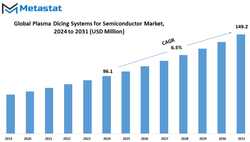
Global Plasma Dicing Systems for Semiconductor market is estimated to reach $149.2 Million by 2031; growing at a CAGR of 6.5% from 2024 to 2031.
GROWTH FACTORS
This will continue to be a growth of plasma dicing systems for the semiconductor market in the coming years. For example, industry faces new areas of challenge and change and several key factors that will transform the industry. The pace at which semiconductor technology is advancing is without an equal in history. With demand for electronic devices that are stronger and more efficient, manufacturers have never stopped pushing the boundaries of semiconductor technology. Plasma dicing systems play a very pivotal role in this procedure. Silicon wafers are cut into minute sized working components through the mechanism of cutting, which is accurate and efficient.
Increasing adoption of plasma dicing systems in various industries is a factor driving the market. With 5G, artificial intelligence, and the Internet of Things getting more mainstream, there has been a consistent requirement for high-performance semiconductors. Plasma dicing systems ensure such semiconductors are quality and dependable, therefore contributing to their rise in popularity in the market.
The market, however, faces significant challenges. High-cost initial expenses that may prove to be a barrier to entry especially for smaller semiconductor manufacturers in terms of using plasma dicing systems will present a significant challenge. Due to expense costs, companies with a small budget will avoid using such systems. The complicated process of plasma dicing system integration into the existing manufacturing flow will also be difficult for most businesses.
While, on the other hand, high growth opportunities likely to be observed in the marketplace in the near future include: the development of more cost-effective plasma dicing technologies has the potential to make systems available to a wider range of manufacturers; innovations in technology are further expected to cut operational costs and improve the efficiency of plasma dicing systems, making them more attractive to businesses.
Further, miniaturization is increasingly becoming a focus point in the electronics industry; thus, more opportunities will be opened to demand advanced plasma dicing systems. As the electronics shrink into smaller sizes and complexity, then their application will begin to require more precise and reliable cutting of the wafer.
High costs and integration challenges will, therefore, act as a roadblock for players, and yet the global plasma dicing systems for the semiconductor market will still see great growth through technological improvements and increased need in the sector. Innovations that can reduce the cost and improve efficiency will create a big opportunity ahead, and it is sure that the market will be dynamic and moving upward in the coming years.
MARKET SEGMENTATION
By Type
The market for plasma dicing systems in the semiconductor industry is rapidly evolving today primarily due to technological developments and increasing demand for precision in semiconductor manufacturing. The market can be broadly classified into two types: Batch Cutting Equipment and Single Cutting Equipment. While both types of products differ in application, each one stands for a separate step in the semiconductor production processes.
In 2023, Batch Cutting Equipment would have a value of $58.3 million. It can cut up to three semiconductor wafers at once. It can be used to increase productivity in high volume production but also maintains quality because it supports processing several wafers at the same time. For large-scale manufacturing, such equipment plays a very important role since their contribution towards efficiency helps lower the cost of semiconductor production.
On the other hand, Single Cutting Equipment, which stood at $32.8 million in 2023, is designed for cutting single wafers. This product is well suited to applications requiring precise high margin wafers and offers flexibility in processing. Although it may not be equivalent in volume to batch processing, attention towards accuracy and adaptability in this makes it a very imperative application in case when careful handling and intensive work is needed. This segment usually addresses niche markets or especially tailored applications in which the prime concern is on quality detailed processing rather than a large volume in quantity.
Looking into the future, the market for both types of machines will probably keep growing. This is because Batch Cutting Equipment will probably find more high-volume production given their effectiveness and cost-saving features. In specialized fields that require accuracy, Single Cutting Equipment will be used more often. Advances in semiconductor technologies coupled with the need for more precise production lines are likely to spur innovations in both pieces of equipment.
The two market segments of plasma dicing systems for semiconductors are Batch Cutting Equipment and Single Cutting Equipment. Both the market segments have unique strengths and applications with respect to varied market requirements in the semiconductor industry. As technology advances and the need for precision increases, both types of equipment will have to meet the requirements of the fast-changing semiconductor market.
By Mobility
The Global Plasma Dicing Systems for Semiconductor market is crucially advancing with advancing technology. Among the productions of devices that slice semiconductor materials through plasma, it can be very broadly categorized under two primary types: Portable and Fixed.
Portable Plasma Dicing Systems are seen to be rather flexible in their use and portable, useful in various settings, best used in applications where mobility is key. The systems enable the semiconductor producer to conduct such accurate dicing functions on site or in a smaller, more versatile environment. The demand for such systems will be driven by the need for adaptability in the production of semiconductors as technology continues to advance. Portable systems will likely evolve to include added functionality that addresses particular dynamic needs in the industry over time.
On the other hand, Fixed Plasma Dicing Systems are designed to be used within established production environments. Those systems are often installed into specific segments within semiconductor manufacturing facilities and are designed for mass production. Stability and consistent performance are important in high volume, so fixed systems deliver that. Moving forward, with the continued upward surge in demand for semiconductors, fixed systems will be an integral component in the production process so that production will be efficient and reliable.
Going forward, the Global Plasma Dicing Systems for Semiconductor market will most likely host both types of systems as they evolve with respect to the demands placed by the industry going forward. The portable systems will evolve in the latest technology, while on the other hand, the efficiency and capacity of fixed systems will be upgraded due to innovations in semiconductor manufacturing processes.
This will essentially be influenced by technological advance as well as changes in practices on manufacturing and in the pattern of demand for semiconductors in the global market. It thus means that both portable and fixed plasma dicing systems will have to adapt to this trend to remain in competition and meet the required demands of semiconductor manufacturers.
Global Plasma Dicing Systems for Semiconductor seems to continue advancing. The categorization of portable and fixed dicing systems owes to the existence of different demands from different sectors, providing specific benefits for each category. On advancing technology on both bases, this ensures that every form of semiconductor production carried out through these systems is always efficient and effective.
By Application
Global Plasma Dicing Systems for Semiconductor market is expected to record significant development, especially concerning the applications in thin wafer and chip segmentation. Plasma dicing is considered an important technology in semiconductor manufacturing, wherein plasma cuts through the semiconductor material with really high precision. This technique ensures that separation processes for semiconductor components are carried out quite efficiently, with minor damage, along with a very good degree of accuracy, which is quite crucial for producing reliable electronic devices.
Thin wafers are increasingly being adopted in the semiconductor industry. Because of continuous advancement in technologies, there will always be demands for thinner wafers; these are frequently used in advanced electronic devices and high-performance applications. Plasma dicing systems are particularly suited to process these fragile, thin wafers. Plasma dicing ensures very high precision processing to handle even the most fragile thin wafers. This is crucial because the manufacturers seek to be able to advance semiconductor technology to better develop smaller, more energy-efficient devices.
Besides thin wafers, another application of plasma dicing systems includes chip segmentation. In chip segmentation, a semiconductor wafer is divided into individual and distinct chips or die. The process is important to make end-products for use in different electronic device applications. Plasma dicing technology actually provides for a clean and precise means of doing this; the resultant defective wafers are less in number, and it brings out more chips per wafer that can be put to use. This is something crucial in a competitive market where a higher yield and efficiency come hand in hand with profitability.
Future prospects of the Global Plasma Dicing Systems for Semiconductor market will continue to innovate and gain momentum with time. With advancement in semiconductor technology, the demand for more accurate and efficient dicing methods is set to increase. Plasma dicing systems, therefore, should transform to meet the demands and possibly new materials and techniques that can make it better. The market demand will also shift for clear reasons in demand with higher performance and form factors in electronics. Pushing higher-performance and smaller-form-factor electronic devices into making use of advanced plasma dicing technologies is the result.
The needs for chip segmentation as well as thin-wafer processing are met by the Global Plasma Dicing Systems for Semiconductors market, therefore it is set to grow. As semiconductor technology advances on, plasma dicing systems would play a very crucial role in the efficient and accurate production of electronic components.
|
Report Coverage
|
Details
|
|
Forecast Period
|
2024-2031
|
|
Market Size in 2024
|
$96.1 Million
|
|
Market Size by 2031
|
$149.2 Million
|
|
Growth Rate from 2024 to 2031
|
6.5%
|
|
Base Year
|
2022
|
|
Regions Covered
|
North America, Europe, Asia-Pacific Green, South America, Middle East & Africa
|
REGIONAL ANALYSIS
The geographical distribution of the global Plasma Dicing Systems market in terms of its use in the semiconductor industry can be segmented into five major regions: North America, Europe, Asia-Pacific, South America, and Middle East & Africa. Each region is different with specific features and growth prospects that impact the Plasma Dicing Systems market.
North America, including the United States, Canada, and Mexico, is another key region in the semiconductor market. The U.S. and Canada have dominant manufacturers of semiconductors and technological companies that will raise the demand for high-end Plasma Dicing Systems. In addition, an increasing electronics industry in Mexico will further fuel growth in regional market. As technology advances, North America is likely to remain one of the significant markets, along with its continued strong innovation base and increasing investments in semiconductor research and development.

European Market
There are two segments under the European market: the UK, Germany, France, Italy, and the Rest of Europe. The value chain in this region is likely to be significantly driven by Germany due to its stable industrial sector and technological advancement. The European Union itself is scheduled to enact various requirements on the establishment of manufacturing bases for electronics and auto sectors that will be at par with UK and France. Advanced Plasma Dicing Systems would be in greater demand to support this local manufacture, which will be a result of efforts from the European Union to cut back dependence on extraneous semiconductor sources.
Most likely to gain maximum growth in the semiconductor market is going to be India, China, Japan, South Korea, and Rest of Asia-Pacific. As China is gaining its footing as a global leader in electronics manufacturing, the demand for Plasma Dicing Systems would be predominant. Japan and South Korea will play a significant role in defining the future of the market because of their technological capabilities and sense of innovation. A strong and growing electronics industry and an effort to become a semiconductor hub in India will further drive growth in the regional market.
South America, with key players like Brazil, Argentina, and the Rest of South America is expected to grow gradually. The region is not up to the pace required by other regions, but investment in technology and electronics manufacturing will continue to be spent which will help to grow steadily in the market.
The Middle East & Africa, including the GCC Countries, Egypt, South Africa, and the Rest of Middle East & Africa, would provide a mixed market picture. While some of the countries are investing in this region, growth in the plasma dicing systems market is likely to grow much lower than in other regions. However, emerging technological initiatives and investments in electronics manufacturing will be positive factors in future growth.
Regional strengths and changing technological requirements will therefore dictate the Plasma Dicing Systems market globally. Overall market conditions and growth potential in each region will be of crucial importance in establishing the overall landscape for this industry.
COMPETITIVE PLAYERS
There is immense scope for the growth of Global Plasma Dicing Systems for Semiconductors as technology and competition are poised to evolve in the future. Leaders in this industry are dominated by KLA Corporation, Panasonic Connect Co., Ltd., Plasma-Therm LLC, Samco Inc., DISCO Corporation, and SUMITOMO PRECISION PRODUCTS Co., Ltd. These firms are doing tremendous innovations that will guide the distribution of semiconductors into new territories.
KLA Corporation stands out for its strong focus on precision and performance. Their advanced plasma dicing systems are designed to offer exceptional accuracy, which is crucial for the production of high-quality semiconductors. As the demand for smaller and more efficient chips grows, KLA Corporation will likely remain in the lead market for such cutting-edge technologies.
Panasonic Connect Co., Ltd. presents extensive experience along with innovation in its plasma dicing systems and reliability and efficiency, which will address growing requirements for the semiconductor industry. The company's goal of integrating advanced technologies will put it on the path to becoming one of the most significant players that will determine the future landscape in this market.
Another large supplier is Plasma-Therm LLC, whose systems are very flexible and efficient in plasma dicing applications. Plasma-Therm's solutions cover wide requirements in semiconductor manufacturing, making it a key contributor to industry innovation. Their ongoing research and developments will bring even more innovations into the plasma dicing technology stream.
Samco Inc. has gained a reputation for high-performance plasma dicing systems that enhance excellent precision and process control. Their systems focus on the dynamic requirements of semiconductor fabrication to always keep themselves competitive in a fast-changing environment. The future advancement in semiconductor technology hangs on maintaining a high standard in which Samco Inc. contributes.
DISCO Corporation is a company offering strong and reliable plasma dicing solutions. Its further efforts on improving the system efficiency with respect to performance will be a core reason for developing a response to the future semiconductor manufacturing demands. Its new plasma dicing technology innovations by DISCO will be likely to drive market trends and compare new records of performance.
Lastly, SUMITOMO PRECISION PRODUCTS Co., Ltd. proposes cutting-edge plasma dicing systems which are innovative and effective. Commitment to high-precision and reliability ensures them as a competitive force in the global semiconductor market. Continuous evolution of technological inputs will propel SUMITOMO into future developments in plasma dicing.
As these industry leaders continue to innovate, the Global Plasma Dicing Systems for Semiconductor market will face a future defined by efficiency, precision, and performance in semiconductor manufacturing. The competitive landscape of the players who are continuously making their mark through these advances and innovations that they are continually making will set new standards and measure up to the future needs of the market.
Plasma Dicing Systems for Semiconductor Market Key Segments:
By Type
- Batch Cutting Equipment
- Single Cutting Equipment
By Mobility
By Application
- Thin Wafer
- Chip Segmentation
Key Global Plasma Dicing Systems for Semiconductor Industry Players
WHAT REPORT PROVIDES
- Full in-depth analysis of the parent Industry
- Important changes in market and its dynamics
- Segmentation details of the market
- Former, on-going, and projected market analysis in terms of volume and value
- Assessment of niche industry developments
- Market share analysis
- Key strategies of major players
- Emerging segments and regional growth potential