

MARKET OVERVIEW
Within the Glass Wafer for Semiconductor Devices market, the industry dynamics are driven by the demand for increasingly smaller and more powerful electronic components. As technological innovation propels the semiconductor sector forward, glass wafers become pivotal in enabling the production of smaller and more efficient semiconductor devices. This market thrives on the perpetual quest for miniaturization and enhanced performance in electronic applications. Glass wafers are an integral component in the production of semiconductor devices like integrated circuits, transistors, and diodes. The silicon semiconductor industry relies heavily on high-quality glass wafers to provide a stable base for manufacturing chips and circuits.
The glass wafer begins as a cylindrical boule made from materials like quartz, borosilicate glass, or aluminosilicate glass. These glass formulations possess high uniformity and chemical stability needed for fabricating electronic components. The boule is sliced into thin discs using specialized saws, then polished down to an optically flat and scratch-free surface. These glass wafers serve as the foundational substrate onto which the active layers of a semiconductor device are deposited.
Before device fabrication, glass wafers undergo extremely thorough cleaning and surface preparation. Steps like solvent cleaning, wet chemical etching, and high temperature annealing remove contaminants and enhance the molecular bonding between the glass and deposited films. The purity and integrity of the glass wafer surface is paramount for enabling proper electrical performance and reliability.
The semiconductor layers such as dielectric insulators, conductors, and photoresist are laid down on the wafer through techniques like molecular beam epitaxy, chemical vapor deposition, sputtering, and lithography. The glass provides mechanical support while these overlying materials are patterned and etched into integrated circuits or discrete components. The flatness and stability of the wafer surface facilitates precision patterning down to nanometer dimensions.
Glass offers key advantages over other wafer materials for electronics manufacturing. It is inexpensive, nonconductive, and optically transparent. The thermal expansion coefficient and melting point of glass pairs well with silicon. Glass allows inspection and metrology of circuits using optical transmission. And glass wafers are easily scaled up to accommodate larger generation chip sizes and increased production volumes.
As semiconductor technology advances into smaller feature sizes and innovative device architectures, glass wafers must keep pace. Manufacturers continually refine glass composition, surface quality, and mechanical strength to meet industry demands. Investment in glass wafer engineering aims to bolster chip yields, processing capabilities, and end-product performance.
With its unique set of chemicals, optical, thermal, and mechanical attributes, glass remains an indispensable material at the heart of modern semiconductor fabrication. As the foundational substrate for microelectronics, the humble glass wafer enables our interconnected digital world of computers, appliances, mobile devices, and cutting-edge electronics.
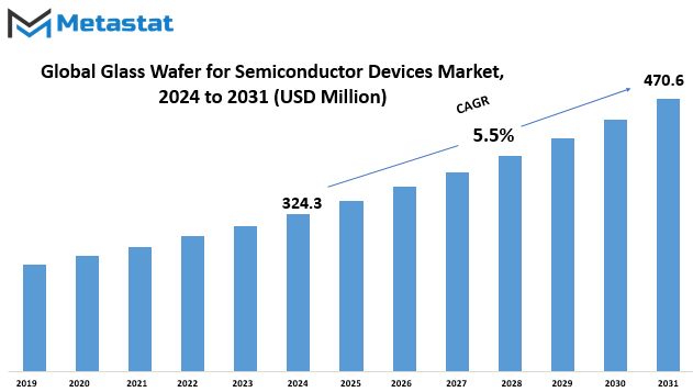
Global Glass Wafer for Semiconductor Devices market is estimated to reach $470.6 Million by 2031; growing at a CAGR of 5.5% from 2024 to 2031.
GROWTH FACTORS
The Global Glass Wafer for Semiconductor Devices market experiences significant growth, driven by various factors that play a pivotal role in its expansion. These growth factors contribute to shaping the market landscape and fostering its development. On the flip side, certain challenges pose potential obstacles to this growth, while emerging opportunities promise to enhance the market’s prospects in the years ahead.
One of the primary drivers propelling the growth of the Global Glass Wafer for Semiconductor Devices market is the increasing demand for advanced semiconductor technologies across various industries. As businesses and consumers alike continue to embrace technological advancements, the need for more efficient and powerful semiconductor devices grows exponentially. This surge in demand acts as a catalyst, propelling the market forward.
Additionally, the continuous innovation and evolution of semiconductor technologies contribute significantly to the market’s expansion. The relentless pursuit of enhancing performance, reducing size, and improving efficiency in semiconductor devices fuels research and development activities within the industry. This commitment to innovation ensures a steady influx of new and improved glass wafers, driving market growth.
On the downside, challenges such as economic uncertainties and fluctuations in global markets pose potential threats to the Global Glass Wafer for Semiconductor Devices market. The market’s susceptibility to economic downturns and unforeseen global events can impact consumer spending and industry investments, thereby hindering the overall growth trajectory.
Moreover, environmental concerns and regulations surrounding the production of glass wafers for semiconductor devices present another set of challenges. As the world increasingly focuses on sustainable practices, industries face pressure to adopt eco-friendly manufacturing processes. Compliance with stringent environmental standards may require additional investments, impacting profit margins and potentially impeding market growth.
Despite these challenges, the market holds promising opportunities that could offset potential setbacks. The growing trend of smart devices and the Internet of Things (IoT) opens up new avenues for glass wafer applications. The integration of semiconductor devices into a wide range of smart products creates a demand for specialized glass wafers, presenting a lucrative opportunity for market players.
Furthermore, the increasing emphasis on 5G technology and its widespread adoption across various regions acts as a significant driver for the Global Glass Wafer for Semiconductor Devices market. The development and deployment of 5G networks drive the need for advanced semiconductor devices, fostering the demand for specialized glass wafers tailored to meet the requirements of 5G technology.
The Global Glass Wafer for Semiconductor Devices market experiences robust growth propelled by factors such as the increasing demand for advanced semiconductor technologies and continuous innovation within the industry. While economic uncertainties and environmental challenges pose potential obstacles, opportunities arising from the surge in smart devices and the adoption of 5G technology promise a bright future for the market. Navigating these dynamics will be crucial for stakeholders aiming to capitalize on the market's growth potential.
MARKET SEGMENTATION
By Type
The Global Glass Wafer for Semiconductor Devices market is categorized based on types, which are further divided into 100mm, 150mm, 200mm, and 300mm. This segmentation plays a crucial role in understanding the diverse landscape of glass wafers in the semiconductor industry.
Glass wafers have become integral components in semiconductor devices, and their usage spans various applications. The categorization by size, with options of 100mm, 150mm, 200mm, and 300mm, offers a nuanced perspective on the market dynamics.
The 100mm glass wafer segment caters to specific requirements where a compact form factor is essential. These smaller-sized wafers find applications in scenarios where space constraints are a critical consideration. Industries that prioritize miniaturization benefit from the compatibility and efficiency of 100mm glass wafers in their semiconductor devices.
Moving up the size spectrum, the 150mm glass wafer segment provides a balanced solution for applications that require a moderate form factor. This size strikes a harmonious equilibrium between compactness and processing capacity. Semiconductor manufacturers often opt for 150mm wafers when seeking a versatile option that accommodates various device functionalities.
The 200mm glass wafer segment signifies a considerable leap in size, offering enhanced processing capabilities. This category is preferred in scenarios where a balance between performance and space utilization is crucial. The 200mm wafers find applications in diverse semiconductor devices that demand a higher degree of complexity in their functionality.
At the upper end of the spectrum, the 300mm glass wafer segment represents a substantial capacity for semiconductor processing. These larger-sized wafers are employed in advanced applications where intricate designs and high-performance specifications are imperative. The 300mm category caters to the evolving needs of cutting-edge semiconductor technologies, providing a platform for pushing the boundaries of innovation.
Understanding the significance of this market segmentation sheds light on the diverse requirements of industries involved in semiconductor device manufacturing. Each size category addresses specific needs, allowing businesses to tailor their choices based on the intricacies of their applications.
The Global Glass Wafer for Semiconductor Devices market segmentation into 100mm, 150mm, 200mm, and 300mm types offers a comprehensive overview of the diverse landscape within the semiconductor industry. The varied sizes cater to different needs, from compact and space-efficient solutions to larger wafers accommodating intricate designs and advanced functionalities. This segmentation is pivotal in navigating the intricate world of semiconductor devices, providing businesses with tailored options to meet their specific requirements and stay competitive in the ever-evolving market.
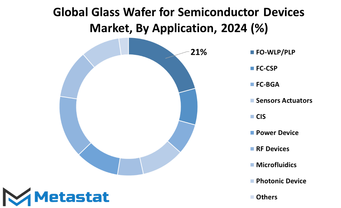
By Application
The Global Glass Wafer for Semiconductor Devices market is segmented based on its applications. These applications encompass FO-WLP/PLP, FC-CSP, FC-BGA, Sensors Actuators, CIS, Power Device, RF Devices, Microfluidics, Photonic Device, and Others.
In examining the market, it becomes evident that various sectors are utilizing glass wafers for their semiconductor devices. This includes the utilization of glass wafers in applications like FO-WLP/PLP, where they play a significant role. Additionally, FC-CSP and FC-BGA applications demonstrate the versatility of glass wafers in meeting the diverse needs of the semiconductor industry.
Sensors and actuators, crucial components in many electronic devices, also find a place in the market segmentation. Glass wafers contribute to the functionality and performance of these components. The same holds for CIS (Contact Image Sensors), where the application of glass wafers is integral to the production of high-quality imaging devices.
Moreover, glass wafers are essential in the Power Device segment, ensuring the reliable and efficient operation of power-related semiconductor components. RF Devices, Microfluidics, and Photonic Device applications further underscore the wide-ranging applications of glass wafers in the semiconductor landscape.
The market's embrace of glass wafers across such diverse applications speaks to the material’s adaptability and effectiveness in meeting the demands of the semiconductor industry. As technology continues to advance, the significance of glass wafers in these various applications is poised to grow, contributing to the ever-evolving landscape of semiconductor devices.
By End-User
The global market for glass wafers used in semiconductor devices plays a crucial role in various industries. When we break down the end-user industries within this market, we find distinct sectors that heavily rely on these glass wafers for their electronic components. These sectors include consumer electronics, automotive, industrial applications, aerospace and defense, and other miscellaneous sectors.
Consumer electronics, as one of the primary end-user industries, showcases a substantial demand for glass wafers. In today's tech-driven world, the production of smartphones, tablets, and other electronic gadgets depends significantly on the quality and efficiency of these wafers. The seamless integration of glass wafers in consumer electronic devices contributes to the overall performance and functionality of these products.
Moving to the automotive sector, glass wafers are increasingly vital components in the manufacturing of modern vehicles. The automotive industry utilizes these wafers for various applications, such as in-car electronics, sensors, and control systems. The reliability and precision offered by glass wafers play a pivotal role in enhancing the technological aspects of automobiles.
In the industrial domain, the usage of glass wafers extends to a wide range of applications. Industries rely on these wafers for sensors, monitoring devices, and other electronic components crucial to their operations. The durability and performance of glass wafers contribute significantly to the efficiency and functionality of industrial processes.
The aerospace and defense sector also stands as a prominent consumer of glass wafers. In this high-stakes industry, precision and reliability are paramount. Glass wafers find applications in various electronic systems within aircraft, satellites, and defense equipment, ensuring the seamless operation of critical technologies.
The category labeled as Other encapsulates diverse industries that utilize glass wafers for their specific electronic requirements. This broad classification highlights the versatility of glass wafers, finding applications in areas beyond the major sectors mentioned.
The global market for glass wafers catering to semiconductor devices caters to a spectrum of end-user industries. Each sector, be it consumer electronics, automotive, industrial, aerospace and defense, or other miscellaneous areas, benefits from the unique properties and functionalities that glass wafers bring to electronic components. As technological advancements continue to shape our world, the demand for these glass wafers across various industries is expected to persist and evolve.
By Glass Material Type
The global market for glass wafers used in semiconductor devices is classified based on different types of glass materials. One prominent category is Borosilicate Glass, which recorded a value of 132.3 USD Million in the year 2023. This type of glass has gained significance in the semiconductor industry due to its specific properties and applications.
Another significant category is Fused Silica Glass, which achieved a valuation of 52.1 USD Million in 2023. Fused Silica Glass holds its place in the market owing to its unique attributes that cater to the requirements of semiconductor device manufacturing.
Quartz Glass is also a key segment in the global Glass Wafer for Semiconductor Devices market, with a valuation of 82.5 USD Million in 2023. The distinctive properties of Quartz Glass make it a preferred choice in the production of semiconductor wafers.
Almino-borosilicate is another noteworthy category, with a market value of 28.1 USD Million in 2023. The semiconductor industry recognizes the specific advantages offered by Almino-borosilicate glass, contributing to its presence in the global market.
Soda-Lime Glass is part of the glass material types considered in this market segmentation. While the specific value for this segment in 2023 is not mentioned, it is acknowledged as a relevant category in the Glass Wafer for Semiconductor Devices market.
These distinct glass material types highlight the diverse nature of the global market, where each category addresses specific requirements in semiconductor device manufacturing. The values associated with each segment underscore their respective contributions to the overall market landscape, reflecting the dynamic nature of the semiconductor industry.
REGIONAL ANALYSIS
The global market for glass wafers used in semiconductor devices is segmented by geography into North America, Europe, and other regions. This segmentation helps in understanding the market dynamics and trends specific to each geographical area. For instance, North America might experience different factors influencing the demand and supply of glass wafers compared to Europe.
Analyzing the market based on geography enables businesses and stakeholders to tailor their strategies according to the unique characteristics of each region. Factors such as economic conditions, technological advancements, and regulatory environments vary across these geographical divisions, impacting the glass wafer market differently.
North America, being a hub for technological innovation, may witness a higher demand for glass wafers due to the flourishing semiconductor industry. On the other hand, Europe, with its diverse economic landscape, might present distinct opportunities and challenges for the market players.
Understanding these regional nuances is crucial for companies operating in the global glass wafer market. It allows them to adapt and respond effectively to the specific needs and preferences of customers in different parts of the world. As businesses navigate the complexities of the semiconductor industry, a geographical perspective provides valuable insights that can drive informed decision-making and foster success in this competitive market.
COMPETITIVE PLAYERS
The global market for Glass Wafers utilized in Semiconductor Devices is characterized by the presence of several key players who contribute significantly to the industry's development. Among these influential entities are Corning Inc., Asahi Glass Co., Ltd, Plan Optik, Tecnisco Ltd, Nippon Electric Glass Co., Ltd., Samtec, Dsk Technologies Pte Ltd, Swift Glass Inc., Nano Quarz Wafer, SCHOTT AG, and WaferPro LLC.
Corning Inc. stands out as a notable player in this market, leveraging its expertise in glass technology to enhance semiconductor device manufacturing. Asahi Glass Co., Ltd, another prominent participant, brings substantial experience to the industry, contributing to the innovation and progress of glass wafers.
Plan Optik, Tecnisco Ltd, and Nippon Electric Glass Co., Ltd. further enrich the competitive landscape with their unique strengths and capabilities. These players not only contribute to the market's growth but also foster healthy competition, driving advancements in Glass Wafer technology.
Samtec, Dsk Technologies Pte Ltd, and Swift Glass Inc. each play a vital role in the industry, bringing their distinct contributions to semiconductor device manufacturing. Their active participation ensures a dynamic environment, promoting continuous improvement and innovation.
Nano Quarz Wafer, SCHOTT AG, and WaferPro LLC complete the roster of influential players in this market. Their commitment to excellence and technological advancements further solidifies the Glass Wafer sector's position in the semiconductor device industry.
The collaboration and competition among these key players create a thriving ecosystem, propelling the Glass Wafer for Semiconductor Devices market forward. As these entities continue to drive innovation and quality in the industry, the market is expected to witness sustained growth and evolution in the coming years.
Glass Wafer for Semiconductor Devices Market Key Segments:
By Type
- 100mm
- 150mm
- 200mm
- 300mm
By Application
- FO-WLP/PLP
- FC-CSP
- FC-BGA
- Sensors Actuators
- CIS
- Power Device
- RF Devices
- Microfluidics
- Photonic Device
- Others
By End-User Industry
- Consumer Electronics
- Automotive
- Industrial
- Aerospace and Defense
- Others
By Glass Material Type
- Borosilicate Glass
- Fused Silica Glass
- Quartz Glass
- Almino-borosilicate
- Soda-Lime Glass
Key Global Glass Wafer for Semiconductor Devices Industry Players
- Corning Inc.
- Asahi Glass Co., Ltd
- Plan Optik
- Tecnisco Ltd
- Nippon Electric Glass Co., Ltd.
- Samtec
- Dsk Technologies Pte Ltd
- Swift Glass Inc.
- Nano Quarz Wafer
- SCHOTT AG
- WaferPro LLC
WHAT REPORT PROVIDES
- Full in-depth analysis of the parent Industry
- Important changes in market and its dynamics
- Segmentation details of the market
- Former, on-going, and projected market analysis in terms of volume and value
- Assessment of niche industry developments
- Market share analysis
- Key strategies of major players
- Emerging segments and regional growth potential


 US: +1-(714)-364-8383


