
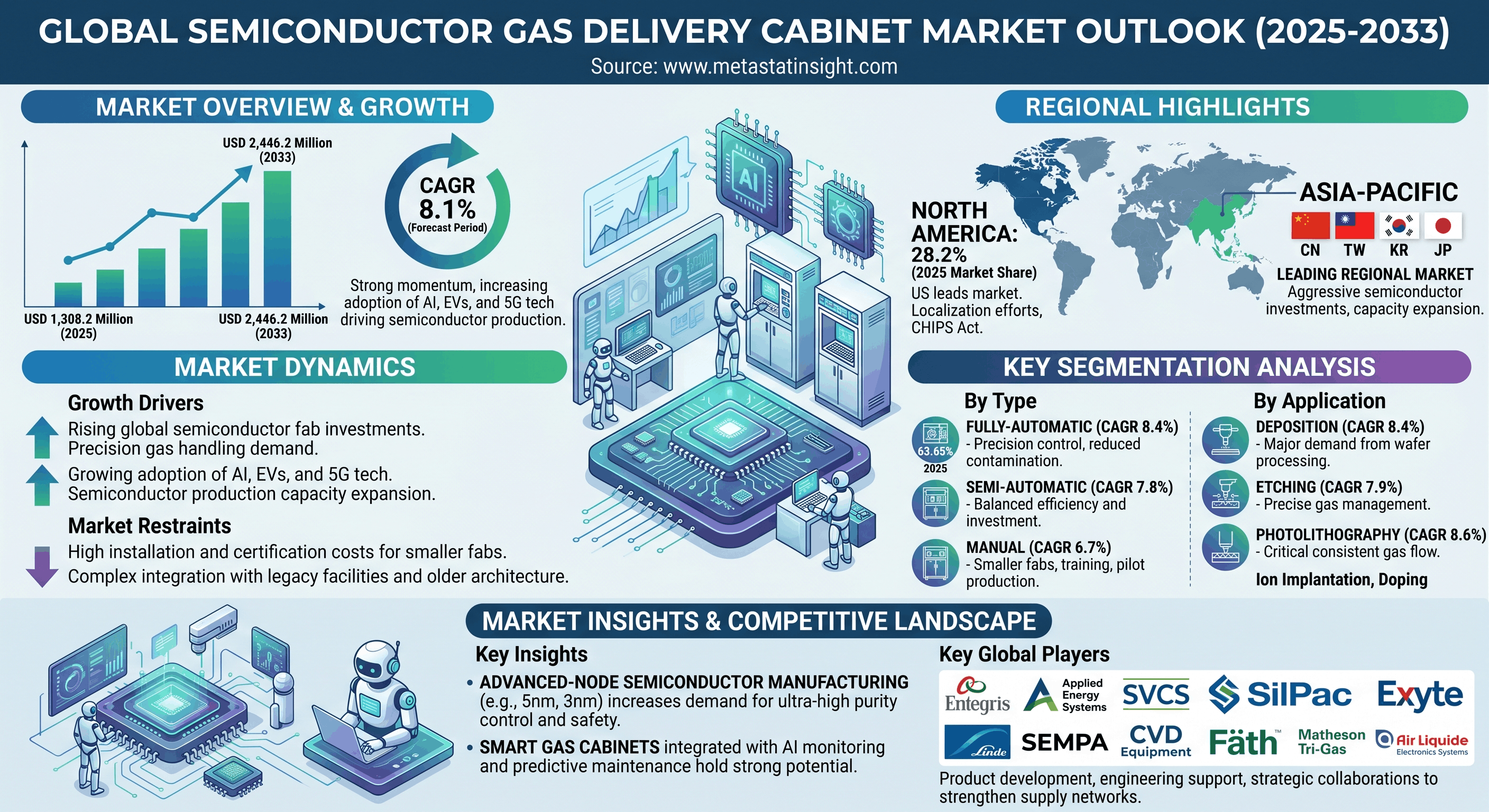
Metastat Insight, a premier provider of comprehensive data-driven market analyses, has published an in-depth strategic outlook on the Global Semiconductor Gas Delivery Cabinet Market. The industry is experiencing remarkable upward traction, with the market valuation projected to grow from USD 1,308.2 million in 2025 to an impressive USD 2,446.2 million by 2033, compounding at a steady CAGR of 8.1% during the forecast period.
Key Industrial Catalyst: The Race for Advanced Nodes
The current momentum across the semiconductor landscape is tied directly to heavy investments in new fabrication facilities globally. As chip architectures shrink toward sub-3nm, 3nm, and 5nm technologies, the demand for ultra-clean, contamination-free processing environments has reached an all-time high. Semiconductor gas delivery cabinets are indispensable in this environment, providing critical, precise regulation and distribution of high-purity specialty gases required for etching, deposition, lithography, and wafer processing.
To maintain strict compliance with tightening workplace safety and environmental regulations, manufacturers are moving away from legacy systems. The market is seeing a rapid shift toward automated solutions outfitted with IoT controls, real-time tracking, leak detection systems, and automated emergency shutoffs to isolate hazardous gases.
Crucial Market Insights & Segment Highlights
-
Dominance of Automation: Fully-automatic gas delivery cabinets are the leading choice for advanced production hubs, accounting for 63.65% of the market share in 2025. This segment is valued at USD 903.5 million in 2026 and is forecast to climb to USD 1,591.9 million by 2033 (8.4% CAGR), driven by the integration of predictive maintenance and smart manufacturing practices.
-
Geographical Leaders:North America holds a 28.2% market share in 2025, with the United States operating as the regional frontrunner. Strategic local policies like the CHIPS Act are currently fueling local fab expansions. Meanwhile, the Asia-Pacific region sustains aggressive facility buildouts in China, Taiwan, Japan, and South Korea.
-
Emerging Geographic Opportunities: Beyond established territories, Southeast Asian nations (including Singapore, Malaysia, Thailand, and Vietnam) and India are transforming into major semiconductor equipment destinations. This expansion is heavily incentivized by government programs and corporate supply-chain diversification.
-
Application Focus: Deposition operations lead the application demands, expected to reach a market valuation of USD 997.1 million by 2033. Photolithography (projected at USD 535.3 million by 2033) and Etching (projected at USD 348.7 million by 2033) follow as primary technical drivers requiring strict gas flow synchronization.
Navigating Market Impediments
While growth prospects remain strong, the report highlights definite operational hurdles. Small and medium-sized chip manufacturing facilities often face adoption barriers due to the capital-intensive nature of equipment procurement, regulatory certifications, and specialized facility setup costs. Additionally, integration remains a complex hurdle when attempting to retrofit legacy, older semiconductor facilities with modern, automated gas infrastructure without disrupting continuous assembly lines.
About the Market Report
The newly released publication tracks historical data from 2021–2025, using 2025 as the base year to formulate strategic projections up to 2033. It offers a micro-level assessment of parent industries, core competencies, changing industrial regulations, and technological shifts across primary global regions including North America, Europe, Asia-Pacific, South America, and the Middle East & Africa.