The global semiconductor ecosystem is experiencing a profound transformation, heavily impacting upstream fabrication consumables. According to a comprehensive data-driven study published by MetaStat Insight, the global Hard Chemical-Mechanical Polishing (CMP) Pad Market is valued at USD 1,227.2 million in 2025. It is projected to expand at a steady Compound Annual Growth Rate (CAGR) of 9.2% during the forecast period, eventually reaching an estimated market valuation of USD 2,479.9 million by 2033.
As integrated circuits become increasingly compact and complex, surface flatness and defect reduction have emerged as vital pillars for advanced chip fabrication facilities worldwide. Hard CMP pads play an indispensable role in ensuring ultra-smooth surfaces during critical wafer processing steps, setting a precise foundation for subsequent lithography, material deposition, and interconnect formation stages.
Driving Forces: The Surge in AI Infrastructure and Node Migration
The robust growth trajectories highlighted in the MetaStat Insight report point toward a structural expansion of advanced semiconductor fabrication facilities and overall wafer processing capacity. Driven by regional supply chain investments, new fabrication plant setups, and aggressive node migration programs, the recurring replacement cycle for polishing consumables remains exceptionally strong.
Furthermore, the exponential adoption of High-Performance Computing (Computing (HPC)), Artificial Intelligence (AI) servers, cutting-edge memory upgrades, and chiplet-based dense packaging formats has catalyzed premium pad demand. The multilayered complexity inherent to next-generation device structures requires absolute precision in planarization, directly boosting the market for highly reliable hard CMP pads.
Key Market Segment Highlights
-
Material Type Leadership: The Polyurethane CMP Pads segment commands a dominant market share of 84.3% in 2025. Valued at USD 1,128.8 million in 2026, it is projected to hit USD 2,126.3 million by 2033, growing at a CAGR of 9.5%. Its strong position is maintained due to structural durability and consistent material removal rates. Concurrently, the Non-polyurethane segment is expected to reach USD 353.6 million by 2033, satisfying niche wafer processes where softer contact is necessary.
-
The Rise of 300mm Wafers: Advanced fabrication facilities are heavily favoring larger wafer form factors. The 300mm Wafer segment is forecasted to lead future volumes, rising at a CAGR of 10.5% to reach USD 1,754.0 million by 2033. Meanwhile, the 200mm Wafer segment remains vital for mature nodes, power devices, and sensors, projected to climb to USD 549.3 million by 2033.
-
Diverse Applications: Logic device manufacturing represents a massive demand pocket, anticipated to reach USD 1,134.8 million by 2033, followed closely by memory devices at USD 899.5 million. MEMS devices are also showing solid progress, positioned to hit USD 236.6 million by the end of the forecast period.
-
Geographical Overview: North America captures a notable 25.8% market share in 2025, led frontally by the United States due to domestic reshoring and government-backed fab investments. Meanwhile, the Asia-Pacific region continues to present vast opportunities, backed by deep-rooted electronics manufacturing clusters and supply chain localization in Taiwan, China, South Korea, Japan, and India.
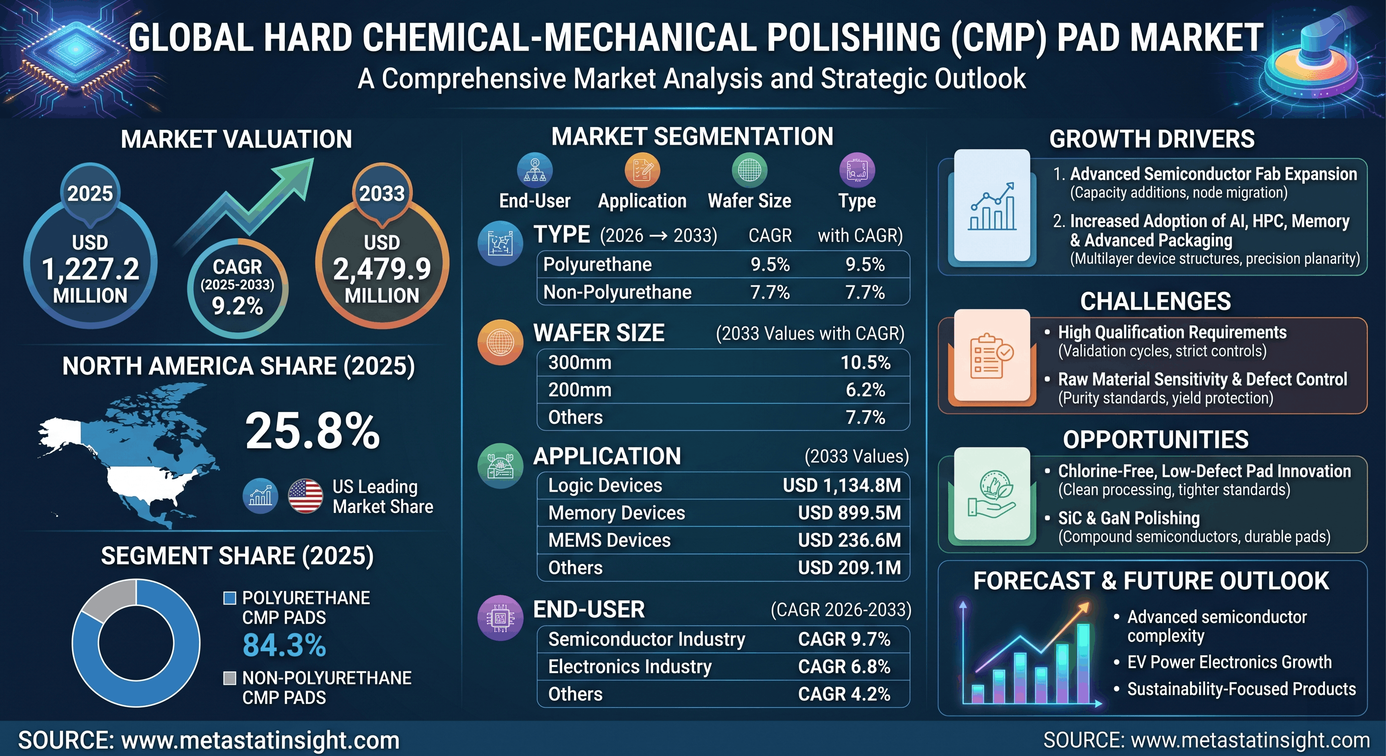
Strategic Hurdles and Future Opportunities
Despite the strong growth curve, manufacturers face intense operational challenges. The industry operates under lengthy validation timelines and strict contamination controls, making process qualification highly fab-specific. Additionally, sensitivity regarding polymer raw materials, particle-induced scratch risks, and constant buyer cost-pressures test supplier margins.
Competitive Framework
The global landscape is highly competitive, consisting of key players that focus on continuous product evolution, uniform slurry distribution, and longer operating cycles to boost fab yields. Prominent market participants analyzed in the research report include NITTA DuPont Inc., Entegris, Inc. (including acquired CMC Materials, Inc.), Hubei Dinglong Co., Ltd., Fujibo Holdings, Inc., IVT Technologies Co., Ltd., SK enpulse Co., Ltd., Pureon AG, 3M, SKC, Alfa Chemistry, FNS TECH Co., Ltd., SPS International, and Topco Scientific Co., Ltd.
About MetaStat Insight MetaStat Insight is a premier market research and strategic consulting firm specializing in deep-dive global industry analyses. By combining rigorous, data-driven methodologies with forward-looking industry insights, MetaStat Insight empowers global enterprises, semiconductor fabricators, and technology stakeholders to navigate market dynamics, optimize supply chains, and make highly informed strategic capital investments.